EUV Lithography Market Overview
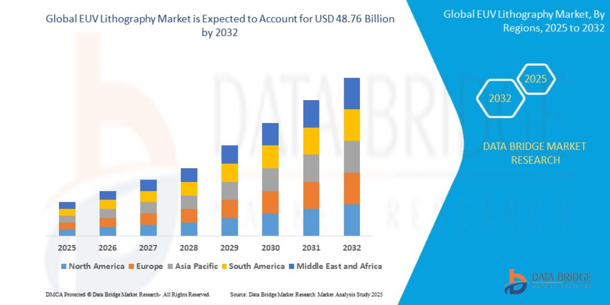
The global EUV (Extreme Ultraviolet) Lithography Market is witnessing substantial growth due to increasing demand for advanced semiconductor manufacturing technologies and the proliferation of high-performance electronic devices. In 2024, the market was valued at USD 11.26 billion and is projected to reach USD 48.76 billion by 2032, growing at a CAGR of 20.10% during the forecast period.
EUV lithography is a cutting-edge technology used in semiconductor fabrication to produce smaller, more efficient, and highly integrated microchips. By using extreme ultraviolet light with a wavelength of 13.5 nm, EUV lithography enables high-resolution patterning, supporting the continued miniaturization of integrated circuits for smartphones, computers, and other electronic devices.
Competitive Landscape
The EUV Lithography Market is dominated by a few key players due to the high complexity and cost of EUV machines. These companies focus on technological innovation, service contracts, and global distribution to strengthen market presence. Major market participants include Cannon Inc. (Japan), ASML (Netherlands), Nuflare Technology Inc. (Japan), SAMSUNG (South Korea), Intel Corporation (U.S.), Nikon Corporation (Japan), SUSS Microtec SE (Germany), Taiwan Semiconductor Manufacturing Company Limited (Taiwan), Ultratech Inc. (U.S.), Vistec Electron Beam GmbH (Germany), Zeiss International (Germany), Toppan Printing Co. Ltd. (Japan), NTT Advanced Technology Corporation (Japan), Toshiba India Pvt. Ltd. (India), and Global Foundries (U.S.).
Request Sample For EUV Lithography Market @ https://www.databridgemarketresearch.com/request-a-sample?dbmr=global-euv-lithography-market
EUV Lithography Market Drivers
Demand for Advanced Semiconductors:
The growing need for high-performance chips in smartphones, IoT devices, AI applications, and automotive electronics is driving EUV lithography adoption.
Moore’s Law and Miniaturization Trends:
As chip manufacturers strive to follow Moore’s Law, EUV lithography allows the creation of sub-7nm and 5nm semiconductor nodes, which are critical for faster and energy-efficient microchips.
Investment in Semiconductor Manufacturing:
Major semiconductor companies are investing heavily in state-of-the-art fabrication facilities (fabs) and EUV tools to enhance production capacity and technological capabilities.
EUV Lithography Market Segmentation
By Node Technology
7nm and Below
10nm–16nm
20nm and Above
By Application
Smartphones and Consumer Electronics
Data Centers and Cloud Computing
Automotive Electronics
AI and Machine Learning Chips
Others
By End User
Semiconductor Manufacturers
Foundries
Integrated Device Manufacturers (IDMs)
BUY NOW @ https://www.databridgemarketresearch.com/checkout/buy/global-euv-lithography-market/compare-licence
Regional Insights
North America is a key market due to advanced semiconductor manufacturing infrastructure, high R&D investment, and early adoption of EUV lithography. The U.S. leads in chip design and fab investments, supporting regional growth.
Europe contributes to the market through research-driven semiconductor initiatives and high-end chip production, particularly in countries such as Germany, France, and the Netherlands.
Asia-Pacific is expected to witness the fastest growth, driven by leading semiconductor manufacturers in Taiwan, South Korea, and China, and the expanding production of high-performance chips for consumer electronics and automotive applications.
Latin America and Middle East & Africa regions are emerging markets with growing demand for consumer electronics, automotive technology, and industrial electronics, which will gradually increase EUV adoption.
EUV Lithography Market Trends
Miniaturization of Semiconductor Nodes:
The push for smaller, faster, and more energy-efficient chips is increasing EUV adoption across advanced semiconductor nodes.
Integration with Next-Generation Electronics:
EUV lithography is critical for AI chips, 5G infrastructure, IoT devices, and autonomous vehicle electronics.
Strategic Collaborations:
Partnerships between equipment manufacturers and semiconductor fabs are enhancing technology deployment and efficiency.
Expansion of Foundries and Fab Capacity:
Increasing investments in high-tech semiconductor fabs are driving demand for EUV lithography machines globally.
Future Outlook for EUV Lithography Market
The EUV Lithography Market Outlooks highly promising, driven by expanding semiconductor demand, adoption of advanced nodes, and technological innovations.
By 2032, EUV lithography is expected to dominate sub-7nm and sub-5nm chip manufacturing, particularly for AI, 5G, IoT, and automotive electronics. Companies focusing on R&D, process optimization, and strategic partnerships will lead market growth, solidifying EUV lithography’s role as a critical enabler of next-generation semiconductor technologies.
About Us:
Data Bridge is one of the leading market research and consulting agencies that dominates the market research industry globally. Our company’s aim is to give clients the knowledge they require in order to function in changing circumstances. In order to give you current, accurate market data, consumer insights, and opinions so that you can make decisions with confidence, we employ a variety of techniques, including surveys, video talks, and focus groups around the world.
Contact :
Data Bridge Market Research Private Ltd .
3665 Kingsway — Suite 300 Vancouver BC V5R 5W2 Canada
+1 614 591 3140 (US)
+44 845 154 9652 (UK)